DAAD Project VIGONI: Combining Fault Tolerance and Offline Test Strategies for Nanoscaled Electronics
01.2007 - 12.2009, DAAD/Vigoni-Project
Project Description
The continuing scaling of circuit technology enables the integration of complete systems and even complete compute clusters on a single chip. At the same time, the nano-electronic structures are subject to a growing number of defect mechanisms. The manu-facturing process is much more sensitive to environmental influences and for very small structures quantum mechanical effects require even higher manufacturing precision. Furthermore, variation in process and material lead to variation in circuit parameters across space (the position on the chip) as well as time (due to ageing effects). The "In-ternational Technology Roadmap for Semiconductors" [SIA] estimates that by 2019 the feature size of process technology will reach 7nm, but only between 10% and 20% of chips will be defect free. In order to achieve economical yield rates, it is imperative that appropriate measures are taken, such as fault tolerance, redundancy, repair and reconfiguration.
In an ongoing trend, the percentage of flip-flops compared to combinatorial elements is growing in modules of free, random logic. This development is a consequence of the massive pipelining used to increase the operation frequency of integrated circuits and of the shorter and shorter critical paths in the combinatorial part. Additionally, many design techniques on architectural level such as speculation and instruction scheduling on the hardware layer, require larger register sets. And finally, the existing techniques for im-proved reliability, such as time and structural redundancy, lead to an increase in the number of memory elements in free random logic. Circuits with millions of flip-flops in free random logic are already commonplace in the industry [Kupp04].
The growth in terms of memory elements is not only observed in data paths but also in control dominated modules, for which regularity and minimized delay is getting more important than minimum area state encoding, which in turn leads to a growing portion of memory elements.
The flip-flops of an integrated circuit are, like its combinatorial elements, subject to the growing variations and the defect and failure mechanisms of nano-electronic circuits, which affect yield during manufacturing as well as reliability during operation. But most significant for flip-flops is their susceptibility with respect to environmental influences, such as particle radiation (e.g. protons), and will require protection mechanisms that im-prove reliability, mask faults and keep a feasible yield. For memory arrays with high re-gularity, there already exist methods that tackle these problems. Some current tech-niques realized in the industry include repair and reconfiguration, error detection and error correction through encoding, periodic refreshment of the data ("scrubbing") to pro-tect from fault accumulation and built-in self-test techniques with redundancy analysis and self-repair.
It will be necessary to adapt these methods to memory structures in free logic, because the growing application of power reduction techniques, such as clock gating, leads to a reduction in the number of concurrently switching elements and especially in concur-rently active flip-flops. Consequently, a large number of flip-flops have to hold their value over a longer time frame, which means, that memory elements are subject to the same long term influences and fault accumulation effects that are already significant for dy-namic memory arrays. Therefore, it is imperative that periodic refreshment is introduced, as is already the case for memory arrays [Hell02].
The susceptibility to transient errors is significantly higher for memory elements than for combinatorial elements [Dodd03]. Because of the ongoing reduction in logic depth, it is expected that masking effects of most combinatorial faults will be reduced and that the soft error rate (SER) even of combinatorial elements will grow by orders of magnitude and approach the SER of unprotected memory elements [Skiv02], and also these effects will result in erroneous states to be detected by appropriate fault tolerance and redun-dancy mechanisms. These techniques are complemented by hardening both combinatorial elements and latches against transient faults.
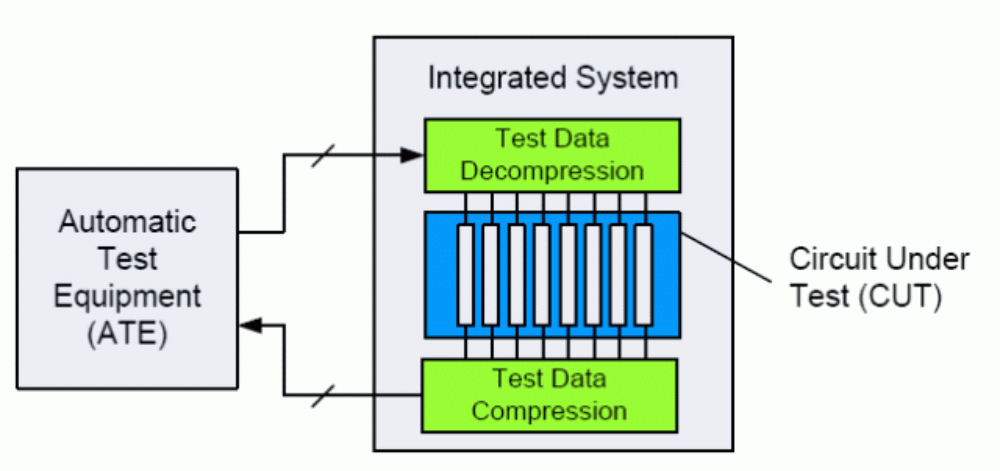
At the same time, the continuous growth in the number of memory elements and the overhead, which is required to improve reliability, make the manufacturing test more dif-ficult which is a dominant cost factor even today. For free logic, scan-path based test is the most wide-spread technique. Here, the test data is being serially shifted into the cir-cuit and read-out, and in order to reduce test time multiple scan-paths are used at once, the test patterns are generated in form of a built-in self test directly on the chip or the test data is provided as a compressed data stream, which is decoded by on-chip cir-cuitry. Similarly the test response is being compressed before it is sent to the tester. Figure 1 shows the basic principle of this embedded test technique.
These compression methods are meant to counter the long imminent problem of manu-facturing test, that the external band-width of a chip to the test equipment is growing much slower than the size of the internal data that is required to achieve a complete fault coverage [Mitr05, Rajs05]. The growing percentage of flip-flops in free random logic and the significant redundancy, employed to increase reliability, aggravate this problem sig-nificantly and would lead to economically unfeasible test lengths and test times, if not accounted for.
The goal of this project is the development of a unified design methodology for memory elements in random logic that combines solutions for reliability, fault tolerance, online and offline test. To achieve this, each scan path (as in Figure 2) is partitioned into seg-ments of a certain length and each segment is extended by redundancy that allows for tolerance or repair of permanent faults in a way that it is still tolerant with respect to tran-sient faults.
A scan path can be seen as a one-dimensional one-bit memory, which lends it to re-spective memory test techniques. For regular memory arrays, periodic test, online test and transparent test have been rigorously analyzed. Some of these test methods can be adapted to the concept of scan paths. But repeated read-out and write-back would sig-nificantly impact availability of the flip-flops to regular system operation and therefore be not feasible. Because of this, it is promising to implement the test technique for trans-parent, periodic self-test, already implemented for memory arrays. A simple logic calcu-lates a residual characteristic (Figure 2), which allows for keeping the contents of the scan path consistent and enables periodic consistency checking.
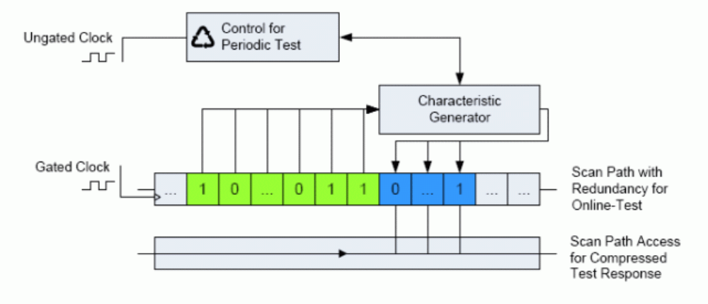
The additional hardware, which is integrated for this online test scheme, will also be used for test response compression. Only the calculated characteristic has to be evalu-ated, from which the incorrect circuit response can be implied. A complete scan-out of the (redundant) circuit response is not required for this solution, and test time is reduced significantly without any additional hardware overhead. For the test pattern (stimuli) the currently known test data compression techniques can still be used.
References:
| [Dodd03] | P. E. Dodd and L. W. Massengill, "Basic mechanisms and modeling of single-event upset in digital micro-electronics", IEEE Transactions on Nuclear Science, 50 (3), pp. 583-602, June 2003 |
| [Hell02] | S. Hellebrand, H.-J. Wunderlich, A. A. Ivaniuk, Y. V. Klimets, and V. N. Yarmolik, "Efficient online and offline testing of embedded DRAMs", IEEE Trans-actions on Computers, 51 (7), pp. 801-809, 2002 |
| [SIA] | Semiconductor Industry Association, "International technology roadmap for semiconductors", Technical Report, 2003, available at: http://public.itrs.net/public.itrs.net |
| [Kupp04] | R. Kuppuswamy, P. DesRosier, D. Feltham, R. Sheikh, and P. Thadikaran, "Full hold-scan systems in microprocessors: Cost/benefit analysis", Intel Tech-nology Journal, 8 (1), pp. 63-72, Feb. 2004 |
| [Mitr05] | S. Mitra, S. S. Lumetta, M. Mitzenmacher, and N. Patil, "X-Tolerant Test Re-sponse Compaction", IEEE Design & Test of Computers, 22 (6), pp. 566-574, 2005 |
| [Rajs05] | J. Rajski, J. Tyszer, C. Wang, and S. M. Reddy, "Finite memory test response compactors for embedded test applications", IEEE Trans. on CAD of Inte-grated Circuits and Systems, 24 (4), pp. 622-634, 2005 |
| [Nico96] | M. Nicolaidis, "Theory of Transparent BIST for RAMs", IEEE Trans. on Com-puter, 45 (10), pp. 1141-1156, 1996 |
| [Koma04] | Y. Komatsu, Y. Arima, T. Fujimoto, T. Yamashita, and K. Ishibashi, "A soft-error hardened latch scheme for soc in a 90nm technology and beyond", Pro-ceedings IEEE Custom Integrated Circuits Conference (CICC'04), pp. 329-332,Orlando, FL, USA, Sep 2004 |
| [Shiv02] | P. Shivakumar, M. Kistler, S. W. Keckler, D. Burger, and L. Alvisi, "Modeling the effect of technology trends on the soft error rate of combinational logic", Proceedings International Conference on Dependable Systems and Networks (DSN'02), Bethesda, MD, USA, pp. 389-398, June 2002 |

Hans-Joachim Wunderlich
Prof. Dr. rer. nat. habil.Research Group Computer Architecture,
retired